VCSEL
GaAs bare substrate
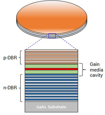
VCSEL epi-wafer
with the MOCVD epitaxial growth process
VCSEL chip fabrication process
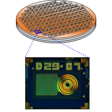
Dicing into single devices or 2D arrays
- The structure of VCSEL epi-wafer consists of a gain media cavity sandwiched by both p-type and n-type Bragg reflectors that have different refractivity values each other to create full mirrors at the bottom and partial mirrors at the top.
- The VCSEL epi-wafer has more than 300 layers of various thin compound semiconductor materials and requires a leading edge crystal growth technology of compound semiconductors with an atomic level accuracy for controlling the desires material composition and thickness of layers in order to have the best electric and optical characteristics of VCSEL chips.
- The VCSEL epi-wafer determines the most of VCSEL chip performances.
- Development and production of the VCSEL epi-wafer require to fulfill extensive qualification requirements and have very high barriers to entry.